Nanometrisis delivers software and consulting services for the characterization of nanostructure morphology and surface topography through the analysis of their microscope images. We are an innovative software company in the fast-growing field of nanotechnology covering the rapidly emergent need for accurate, reliable and targeted metrological characterization of nanotechnology products. Nanometrisis is a spin-off company of the Institute of Nanoscience and Nanotechnology of NCSR Demokritos
- Motivation
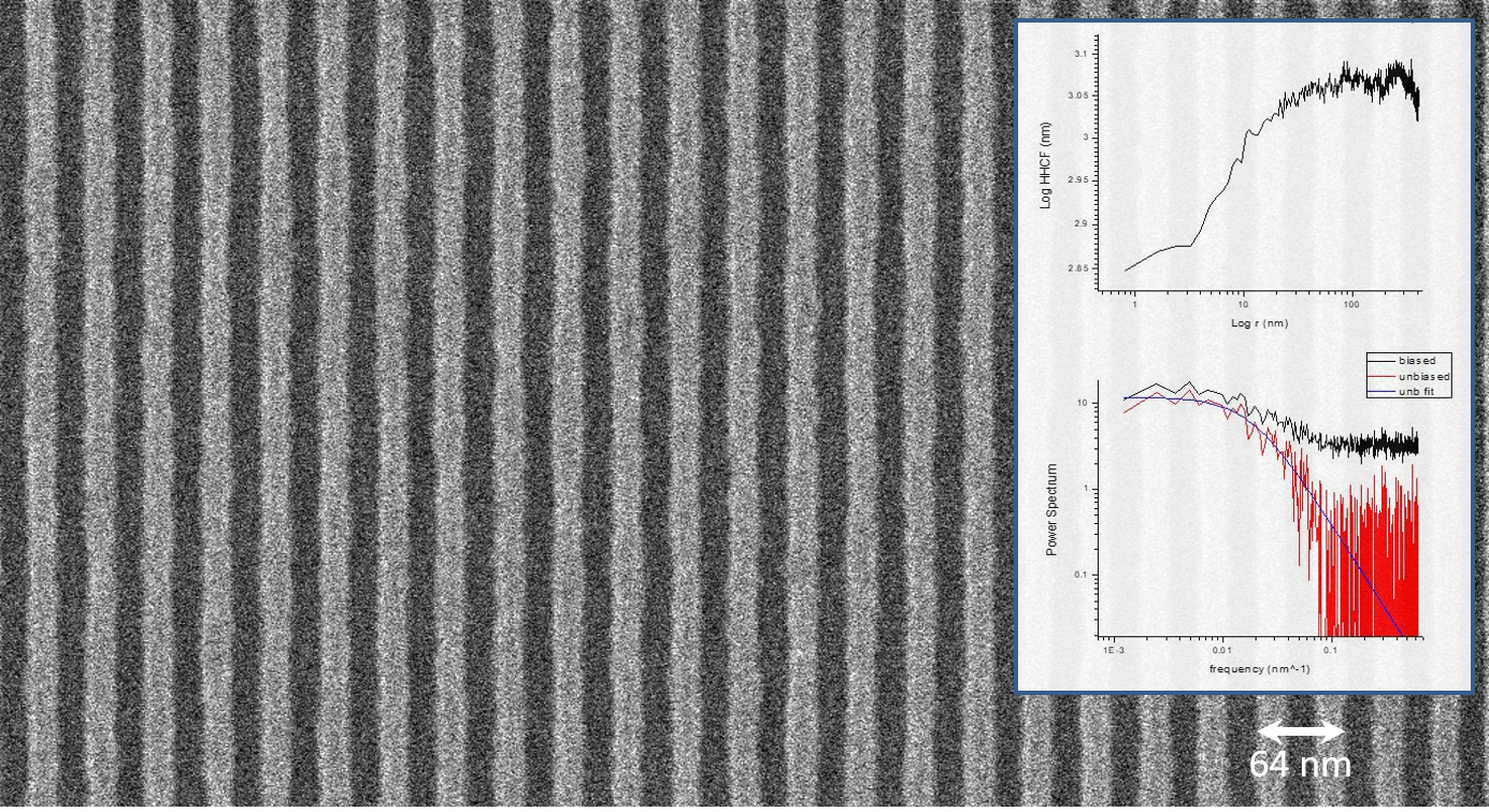
When fabricating something very small, process engineers need to “see it” to know whether it meets the design requirements. Very powerful microscopes are able to deliver high qualify picture of nanosize products. Very often, however, the eye-inspection of microscopic images is not sufficient: a quantitative or mathematical description is required. This is particularly true in nanotechnology, where the properties of nanostructures are often determined by the dimensions and morphology / topography. For example, the microprocessors in cell phones and computers depend critically on the dimensions and roughness of their nanotransistors.
Nanometrisis software family characterizes the size, topography, roughness and morphology of nanostructures from the analysis of microscopy images. It enables manufacturers and users of nanostructures to better assess quality in a broad range of applications of material science and engineering such as electronics, photonics, biology, medicine.
- Innovation
The excellence and innovation of Nanometrisis is summarized in the following points:
Mathematical innovation: Advanced mathematical tools for full description of nanostructures and nanotechnology product surfaces.
The topography and morphology of nanostructures are often highly complex. Complexity is often increased due to the coexistence of random and quasi-organized surface features. The complete and quantified description of this complexity cannot be done with existing mathematical methods. Mathematical innovation is required that will lead to new solutions. Nanometrisis pioneers the development of new mathematical solutions for fuller description of morphological complexity of nanostructures.
Synchronization with industry needs: Prompt adjustment with the roadmaps of the various disciplines of nanotechnology.
The semiconductor and microelectronics industry was the first to establish with great success, roadmaps (every two years) for product and technology development including their metrology (International Technology Roadmap for Semiconductors). This defined directions for the industry, but also quantified the progress to be achieved in the coming years. Nanometrisis closely monitors any changes in these roadmaps and adjusts its software accordingly.
Synchronization with research needs: Continuous feedback with recent research developments and their selective application into further development of software.
The evolution of modern industry is heavily dependent on research focusing on the micro and nanoscale modification and quantitative characterization of its products. Nanometrisis adapts its software incorporating selective and useful new research results thanks to the advanced research experience of its members.
Hybrid (Holistic) Metrology: Algorithmic support of combining measurements from scanning electron (SEM), atomic force (AFM), and other microscopes.
No metrological technique is perfect. Certain inaccuracies or systematic errors may be present in one method, but absent from another one. This weakness is critical if only one technique is used to describe the desired properties of nano products. Hybrid metrology suggests the intelligent combination of two or more measurement methods aiming at minimizing the impact of metrological inaccuracy. Nanometrisis develops an algorithm combining measurements from atomic and electron microscopy for the most precise characterization of roughness and morphology of a free surface.
«Smart» Metrology: Targeted selection of critical parameters for nanostructure characterization depending on their application.
Nanostructured products are usually targeted towards a specific application – e.g. nanoelectronics, optics, wetting control -. However, until now their metrology provides a generic set of parameters and functions regardless of whether such parameters are critical for the specific application. Nanometrisis pioneers a process of targeted (“smart”) metrology, which will guide the user towards those parameters and functions that are most critical in the context of specific applications. This is done on the basis of laws and relationships from theory, simulation and experimental measurement results published in the literature and connecting topographical features with performance in a specific application.
Integration of machine learning techniques in our software.
Nanometrisis develops state of the art deep learning techniques for microscope image enhancement and denoising.
- Advanced Materials, Nanotechnology & Devices
NCSR DEMOKRITOS
Patr. Gregoriou E' & 27, Neapoleos str.
153 41, Agia Paraskevi
Attica, Greece